Technical Process Analysis of Side-lighting Transparent LED Display
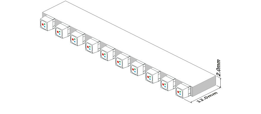
The side-illuminated lamp bead technology is derived from the LCD backlight. It is a niche product in the display industry, with fewer package manufacturers, different quality, and poor color consistency.
PCB strip width * thickness is 8.0mm * 3.0mm, the side view angle of the screen to see the degree of transparency of the general performance.
The minimum resolution can only achieve P3.2, and the adjacent lamp bead chips interfere with each other, and the color deviation of the whole screen is large.
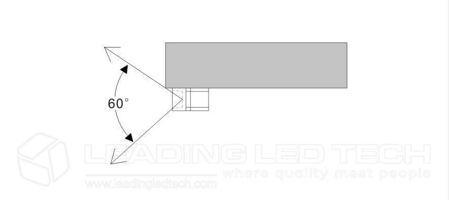
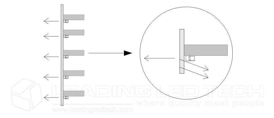
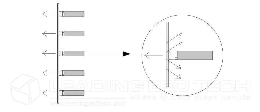
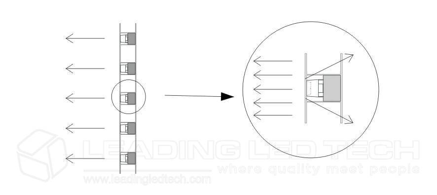
The LED lamp bead has an uneven illumination angle, and the viewing angle in the up and down direction is only 60 degrees.
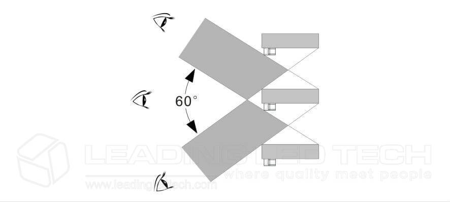
Viewed from a 60-degree angle of view, the product will appear as a grid phenomenon.
The LED pads are arranged in a line on the back of the lamp bead, and the force is uneven, which is prone to falling off.
Due to the poor protection of bare light strips, the damage rate of the lamp to the lamp during transportation is relatively high.
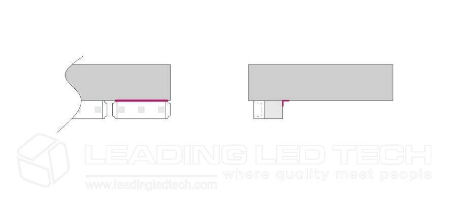
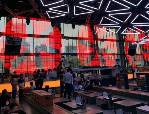
In order to improve product protection, an acrylic panel is added in front of the transparent screen, and the lamp bead is reflected by the panel to the back of the screen body, and the back of the screen body is affected by light pollution.
______________________________________________________________________________________________________________________________________
Technical Process Analysis of Front-lighting Transparent LED Display
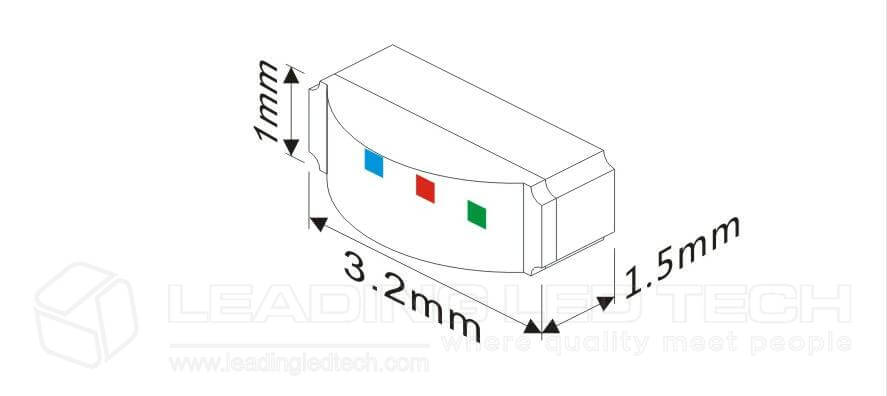
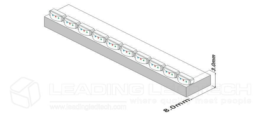
It adopts the conventional outdoor SMD-LED lamp beads in the industry, and the commonly used models are 1921, 2121, 3535 and so on.
PCB strip width * thickness is 12mm * 2.8mm, the effect of the front view angle is better, the side view viewing screen body permeability is relatively low.
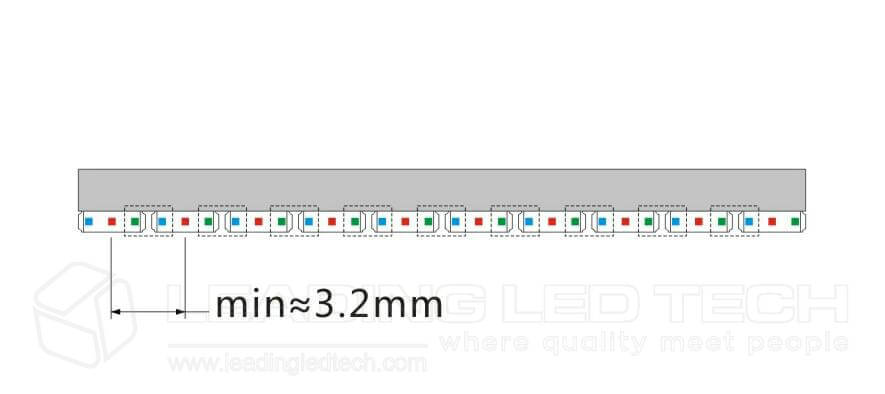
The minimum size of the lamp bead can be 2.0mm, and the minimum resolution of the transparent screen can be around P2.5.
The LED lamp bead has a uniform illumination angle and a full viewing angle of about 140 degrees.
In the case of a 60 degree viewing angle, a grid phenomenon will appear on the screen.
The LED pads are located at the four corners of the lamp bead. The pad size is narrow and the lamp bead is not firmly soldered, which is prone to lamp beading or soldering.
Due to the poor protection of bare light strips, the damage rate of the lamp to the lamp during transportation is relatively high.
In order to improve product protection, an acrylic panel is added in front of the transparent screen, and the lamp bead is reflected by the panel to the back of the screen body, and the back of the screen body is affected by light pollution.
______________________________________________________________________________________________________________________________________
Technical Process Analysis of GOB Transparent LED Display
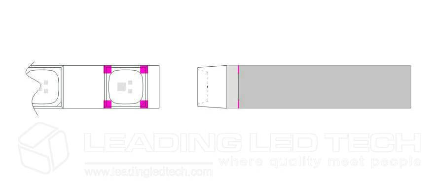
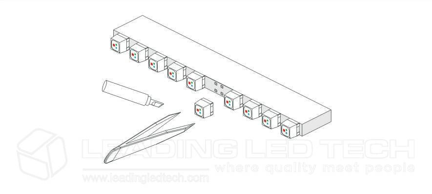
Adopt the industry’s conventional SMD LED lamp beads, models are 1921, 2121, 2727, 3535, etc.
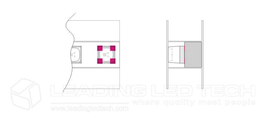
PCB strip width* thickness reaches 6.0mm*3.0mm, and the side view angle of the screen is relatively low.
The minimum size of the lamp bead can achieve 2.0 password, and the minimum resolution of the transparent screen can only be about P2.5.
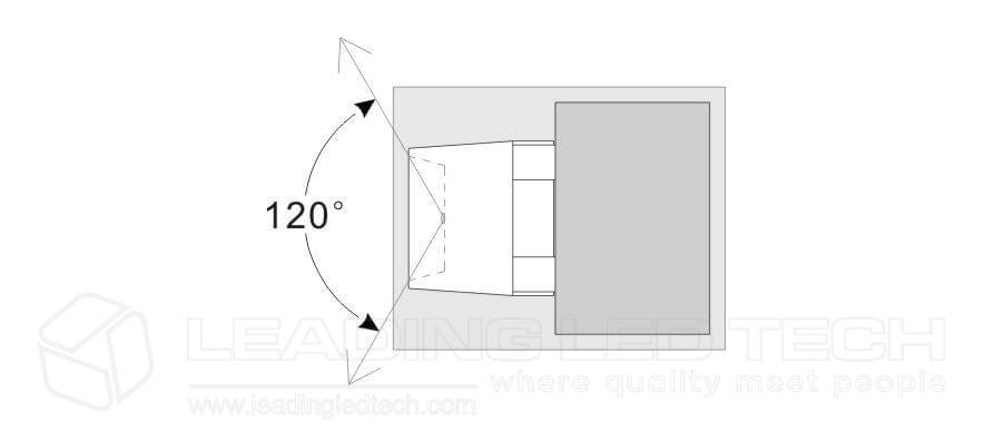
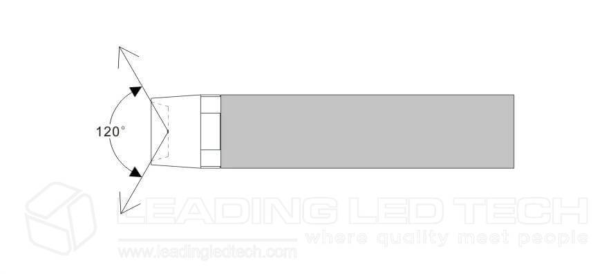
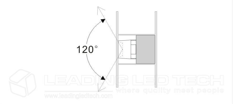
The LED lamp bead has a uniform illumination angle and the full viewing angle is only 120 degrees. However, due to the interference of the sealing glue, the viewing effect is different at different angles.
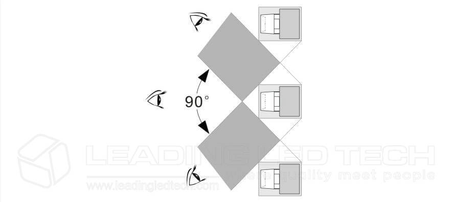
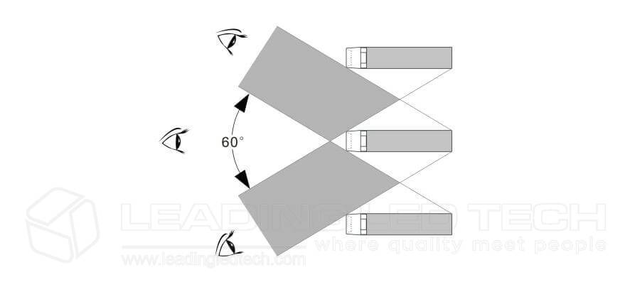
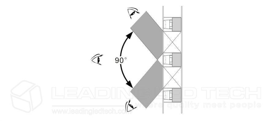
The size of the light bar is wide, plus the visual interference of the sealant. When the viewing angle is 90 degrees, the product has a grid phenomenon.
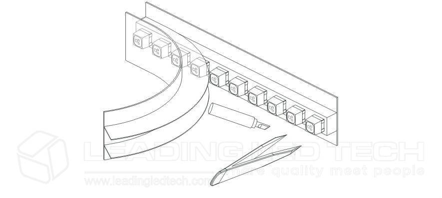
The LED lamp bead is sealed in the middle of the resin, and then the CNC is cut. The side of the light bar is prone to gaps and the protection performance is normal.
When repairing the LED lamp bead, it is necessary to remove a large amount of resin around the abnormal lamp position, and the maintenance cost is high.
There is resin in front of the LED lamp bead. When the display is in use, the lamp bead is reflected by the resin to the back, and there is light pollution on the back of the display.
______________________________________________________________________________________________________________________________________
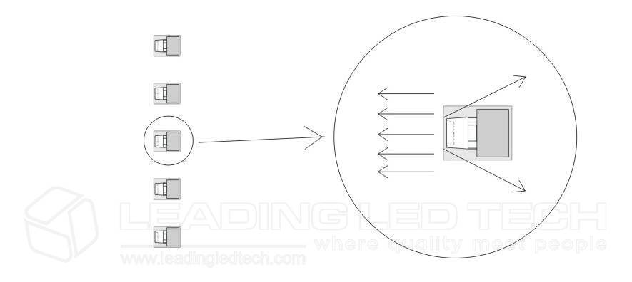
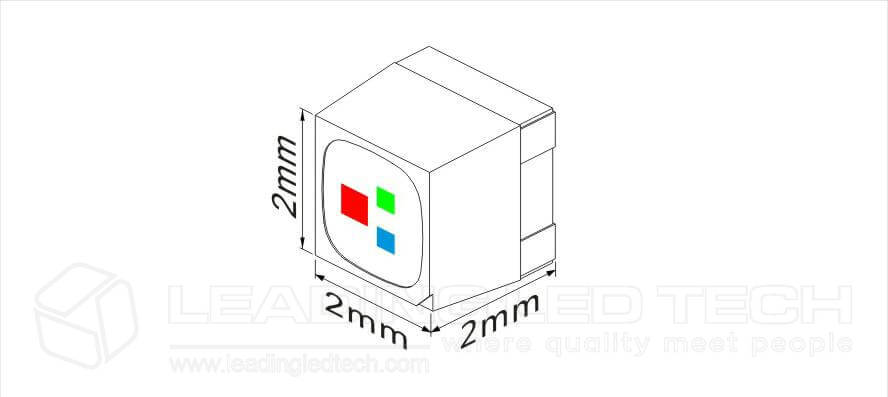
Technical Process Analysis of COB Transparent LED Display
![]()
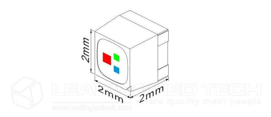
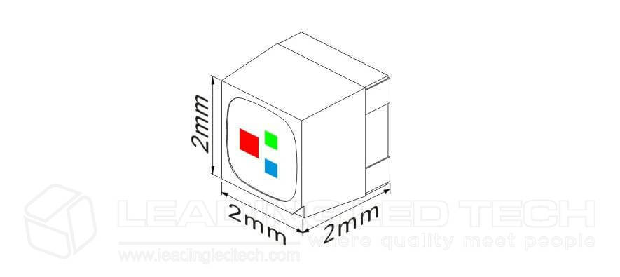
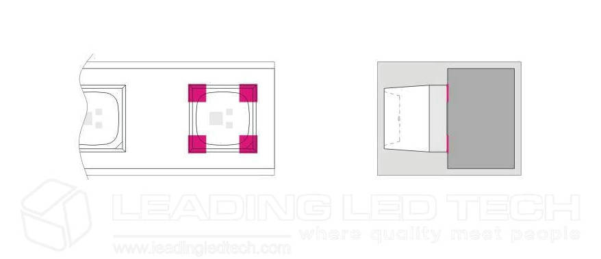
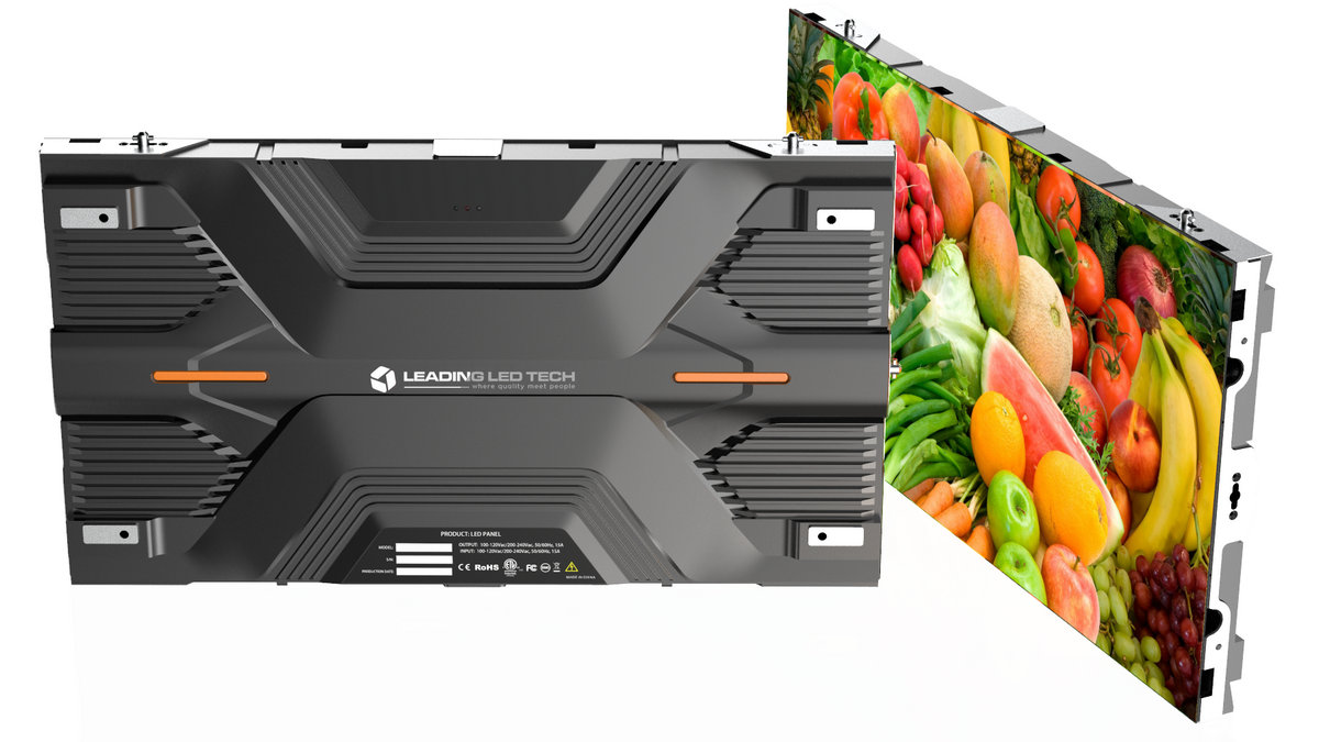
It adopts COB(chip on board) professional package, the lamp bead height is 0.4mm, the diameter is 2mm, the lamp bead is good in protection and the maintenance probability is low.
![]()
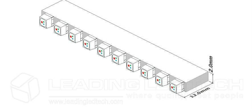
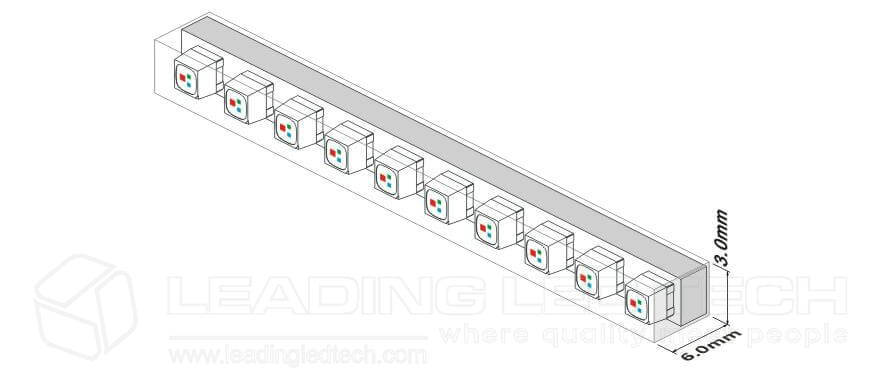
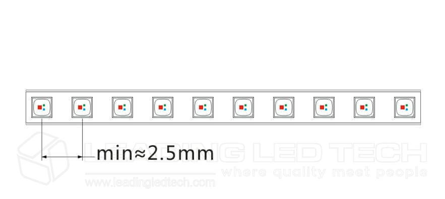
PCB strip width* thickness is only 2.5mm*3.0mm, and the transparency of each viewing angle of the screen is extremely high.
![]()
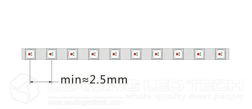
The minimum diameter of the lamp bead can be 0.4mm, and the minimum resolution of the transparent screen can be around P1.0.
![]()
The LED lamp bead is evenly illuminated, and the full viewing angle reaches 180 degrees. The viewing angle of the transparent screen is the same from any angle.
![]()
The light bar is small in size and can be viewed from a large viewing angle of 160 degrees.
![]()
The LED pad is sealed in the middle of the resin, and the glue seal around the light bar is sealed, and the light bar is excellent in protection.
![]()
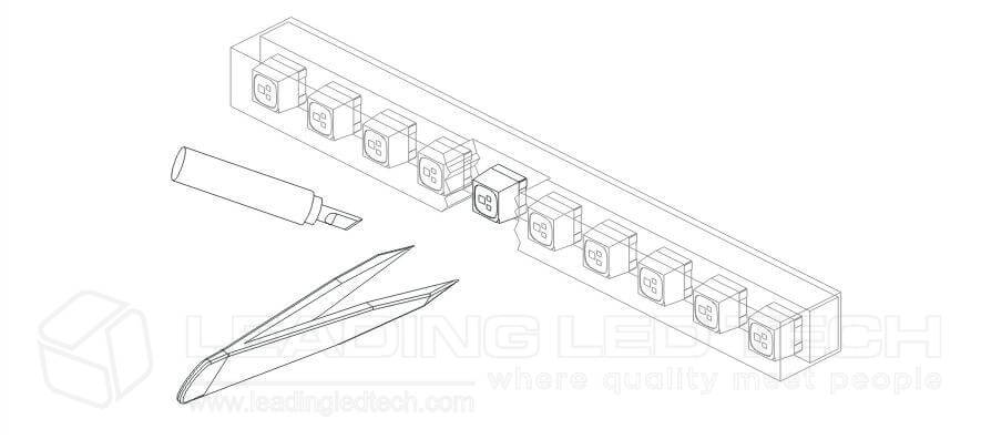
When repairing the LED lamp bead, only a small amount of resin in the abnormal lamp position needs to be removed, the amount of glue taken is small, the maintenance is convenient, and the maintenance reuse rate is high.
![]()
The LED lamp bead does not require any protective mask, the lamp bead shines directly, and there is no light pollution on the back of the display.
______________________________________________________________________________________________________________________________________
Technical Process Analysis of Laminating Transparent LED Display
Adopt the conventional SMD LED lamp beads in the industry, common models 1921, 2121, 2727, 3535 and so on.
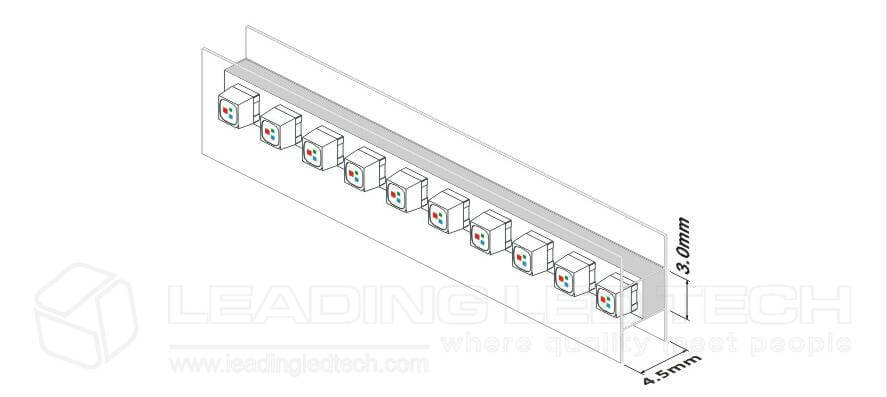
PCB strip width* thickness reaches 4.5mm*3.0mm, and the transparency of the screen is low while viewing from the side.
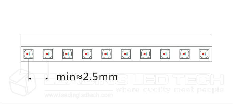
The minimum size of the lamp bead can be 2.0mm, and the minimum resolution of the transparent screen can only be about P2.5.
The illumination angle of the lamp bead is uniform, and the full viewing angle is about 120 degrees. However, due to the interference of the film, the effect of viewing at different angles is different.
The strip size is wide, and with the interference of the film, the grid phenomenon appears when the viewing angle is 90 degrees.
The LED lamp beads are only adsorbed in the middle of the two layers of the film before and after, and the adsorption force is uneven, and the protection is poor.
When the LED lamp bead is repaired, the double film of the entire module needs to be torn open, and the maintenance cost is high.
There is a film in front of the LED lamp bead. When the display is in use, the lamp bead is reflected to the back through the film, and there is light pollution on the back of the display.
Leave A Comment
You must be logged in to post a comment.